Key words diamond, grinding wheel, wire saw|2020-06-15 09:48:35|source super hard material foundation
1. Processing of monocrystalline silicon and polycrystalline silicon
Monocrystalline silicon and polycrystalline silicon
Monocrystalline silicon is a relatively active non-metallic element. This crystal has a substantially complete lattice structure and is a good semiconductor material with a purity of 99.9999%. It is mainly used for manufacturing semiconductor devices and solar cells. The manufacturing method of single crystal silicon (Figure 1a) is usually to first produce polycrystalline silicon or amorphous silicon, and then grow a rod-shaped single crystal silicon from the melt by the Czochralski method or the floating zone melting method. Polycrystalline silicon (Figure 1b) is a form of elemental silicon. When molten elemental silicon solidifies under supercooled conditions, silicon atoms are arranged in a diamond lattice into many crystal nuclei. For example, these crystal nuclei grow into crystals with different crystal plane orientations. Grains, and these grains combine to crystallize into polysilicon. Polycrystalline silicon is the direct raw material for the production of monocrystalline silicon, and it is the basic material of electronic information for semiconductor devices such as artificial intelligence, automatic control, information processing, photoelectric conversion and so on. Known as "the cornerstone of the microelectronics building".

Figure 1 Monocrystalline silicon and polycrystalline silicon
Processing flow The processing flow of single-crystal silicon mainly includes the steps of truncation-rounding-cutting-square grinding-slicing-chamfering-grinding-chemical etching-polishing. In contrast, polysilicon does not have the steps of cutting and spheronization. It only needs to cut the square and slice after the preparation of the ingot. In the entire process of preparing single crystal silicon and polycrystalline silicon from ingot to chip, diamond tools with different uses are required to participate in the processing, such as diamond circular saw blades, band saws, high-precision grinding wheels, wire saws, ultra-thin slices, etc., and processing The accuracy requirements are relatively high.
2. Sapphire processing
The composition of sapphire is Al2O3, the Mohs hardness is 9, second only to the hardness of superhard materials. Due to its superior light transmission performance and wear resistance, it is mostly used in the base of LED light-emitting components, optical windows, and watch cases of high-end watches. And mobile phone cameras. Sapphire has the characteristics of being hard and brittle, and it is expensive. In the process of processing, high precision, fast processing efficiency, low material loss and clean working environment are generally required. Diamond is the material with the highest hardness and the highest wear resistance in nature, so diamond tools are the best choice for processing sapphire materials.

Figure 2 Sapphire wafer
The processing flow is from sapphire ingot to the final substrate (Figure 2). The main flow includes the following steps: crystal growth—drawing rod—rolling—ingot orientation—slicing—grinding—chamfering—polishing, each step needs to be equipped Different diamond tools are used to complete, the main tools are diamond sleeve bit, diamond grinding wheel, diamond wire saw, etc.
3. Diamond Tools
1. Diamond Wire Saw
At present, the most popular research is the diamond wire saw (Figure 3). Asahi Diamond and Nobu Takeshi of Japan, Saint-Gobain of France and diamond wire tech of the United States have all done a lot of research on the diamond wire saw and have launched their own Products; There are already many large-scale production enterprises of diamond wire saws including Yang Ling Meichang, Changsha Dell, Nanjing Sanchao, Qingdao Gaoche, etc. Diamond wire saws are also widely used in the preparation of monocrystalline silicon, polycrystalline silicon and sapphire And slice, and the market demand is huge. In 2017, there was a hard-to-find situation in China.

Figure 3 Diamond wire saw
The parameters and applications of diamond wire saw are shown in Table 1.

With the application and development of large-size silicon wafers and sapphire wafers, the diamond wire saw will be used as a cutting tool for new-generation silicon wafers and sapphire wafers. Its processing surface has less damage, small deflection, thin slices, and good thickness consistency. It can cut large-size silicon/sapphire ingots, saving materials, high efficiency, large output and high efficiency. This series of unparalleled advantages will be highly valued by silicon wafer and sapphire processing enterprises.
2. Diamond ultra-thin scribe

Figure 4 Diamond ultra-thin scribe
The ultra-thin dicing blade (Figure 4) is composed of diamond and binder in the form of a ring-shaped sheet with a thickness between 0.015 and 0.3 mm. The thickness of the metal bond electroplating blade is 0.015mm to 0.1mm, and the thickness of the metal bond hot pressing blade and the resin bond blade is 0.1mm to 0.3mm. Ultra-thin dicing is widely used in the electronics industry to cut or slot various hard and brittle materials, such as silicon, germanium, gallium phosphide, gallium arsenide, gallium arsenide phosphorus, ferrite, lithium niobate, tantalum acid Lithium, piezoelectric ceramics, optical ceramics, glass, etc.; It has the characteristics of high cutting accuracy, narrow slits, long service life, etc.; it needs to be installed on special equipment when it is used, and it can be used by single knife or multiple knife at the same time. According to information, annual sales of ultra-thin scribing in the world amount to more than 500 million US dollars. At present, the market for such products is mainly monopolized by world-leading companies such as Japan and the United States. The tools produced by these companies have stable performance, complete specifications, and high cutting accuracy. my country's electronics industry is entering a period of rapid development, and the demand for precision cutting tools has also entered a period of rapid growth. However, due to the late development of this type of product in China, there are still many defects in its performance, which cannot meet the requirements of the rapid development of the domestic market. Therefore, a large number of various types of scribing are imported from abroad every year. In China, there are few companies that research and manufacture thin grinding wheels and enter the market. Therefore, the research and development of ultra-thin dicing blades have broad market prospects.
3. High precision diamond wheel

Figure 5 Diamond wheel
Diamond grinding wheels are the most widely used in the processing of hard and brittle materials such as crystalline silicon and sapphire. From the processing of the ingot to the rough processing of the wafer to the finishing, different types of diamond grinding wheels are used; mainly including the ingot Spherical grinding wheel (Figure 5a), plane grinding wheel (Figure 5b), thinning wheel (Figure 5c) and polishing wheel (Figure 5d), etc., the diamond particle size is from 250# to 8000#, the carcass material includes metal base, Resin-based and ceramic-based. The purpose of silicon wafer grinding is to remove saw marks and surface damage caused by slicing, effectively improve the warpage, flatness and parallelism of silicon wafers, and reach the specifications that can be handled by a polishing process. When grinding silicon wafers, it is important to control the size and uniformity of the cracks. Monocrystalline silicon is a hard and brittle material, which is ground. The abrasive has rolling and micro-cutting effects. The destruction of the material is mainly micro-crushing. The ideal surface shape after grinding is required to be uniform and free of countless micro-cracks. Glossy surface. Grinding can use 350# ceramic-based diamond grinding wheel, the roughness of the processing surface is about 0.5μm, and the diameter of the grinding wheel is usually Φ200mm~Φ350mm. The purpose of polishing is to improve the surface micro-defects of the single crystal silicon wafer to obtain the wafer surface with extremely high flatness and extremely small surface roughness value, and it is required that the surface has no modified layer and no scratch. Polishing method: rough polishing, removing the damaged layer, the general removal amount is about 10μm~20μm, resin grinding wheels with a particle size of 1000#~2000# can be used; fine polishing, improving the roughness of the wafer surface, the removal amount is about 1μm, so that The roughness of the crystal surface can reach 0.3μm, and a diamond wheel with a particle size of 8000# can be used.
4. High precision sleeve bit
Set bit (Figure 6) The processing object is sapphire and other expensive hard and brittle materials, which are mainly used for the processing of watch cases, optical glass and LED substrates. The precision of the bit is very high, with extremely high added value, and the market The demand is increasing year by year, and it has a broad application prospect.

Figure 6 Sapphire drill bit
The manufacturing technology of nested drill bits includes the manufacturing technology of ultra-thin ring bit, high-precision welding technology and subsequent grinding technology of drill bit; the quality of ultra-thin ring bit plays a decisive role in the final performance of the product. Including uniform mixing, fine granulation, standardized hot-press sintering, demoulding and other production processes and operating standards; high-precision welding technology is a key step to ensure the drill bit concentricity and welding strength, including welding surface treatment, welding concentric adjustment, Standardized welding; the role of subsequent grinding of the drill bit is to further improve the accuracy of the drill bit.
5.CMP dresser
With the rapid development of the semiconductor industry, the size of electronic devices has shrunk, requiring wafer surface flatness to reach the nanometer level. Traditional flattening technology can only achieve local flattening, but when the minimum feature size reaches below 0.25 μm, global flattening must be performed. At present, the only technology that can achieve global planarization is mechanical chemical polishing (CMP), which uses chemical etching and mechanical force to smooth the silicon wafer or other substrate materials during processing.
The working principle of CMP is to fix the silicon wafer at the bottom, and then place the polishing pad on the grinding disk, and the polishing liquid composed of submicron or nano abrasive particles and chemical solution flows between the surface of the silicon wafer and the polishing pad; The rotating polishing head is pressed against the rotating polishing pad with a certain pressure to planarize the silicon wafer. The polishing pad is a consumable item, generally made of polyimide material of porous material. The surface of the polishing pad must be regularly trimmed with a diamond trimmer to increase the life. This trimmer is a CMP trimmer. The role of the CMP dresser is to sweep the surface of the pad to improve the surface roughness and remove the used slurry. The dresser contains a stainless steel disc and a nickel-plated (CVD diamond layer) diamond abrasive grain. The grain size of the diamond abrasive grain is about 20 μm (Figure 7).

Figure 7 CMP dresser
3M Company occupies the main market of CMP conditioners. The polishing pad dresser is used for dressing the shape of the polishing pad. The research on the dresser focuses on the dresser size, diamond particle size, diamond particle density, arrangement method, bonding method, etc.; the bonding method of diamond particles is the main research The content requires that while ensuring the life of the dresser, there is no drop of diamond particles, so as not to cause scratches on the wafer.

-All diamond tools can be ordered and fabricated!
- Henry Wang | Quote Manager
-WhatsApp:+86-13459035657
-Email: ceo@zdiamondtools.com
-Web www.zdiamondtools.com
Company Profile

Certifications
Company Team

Exhibition
Logistics

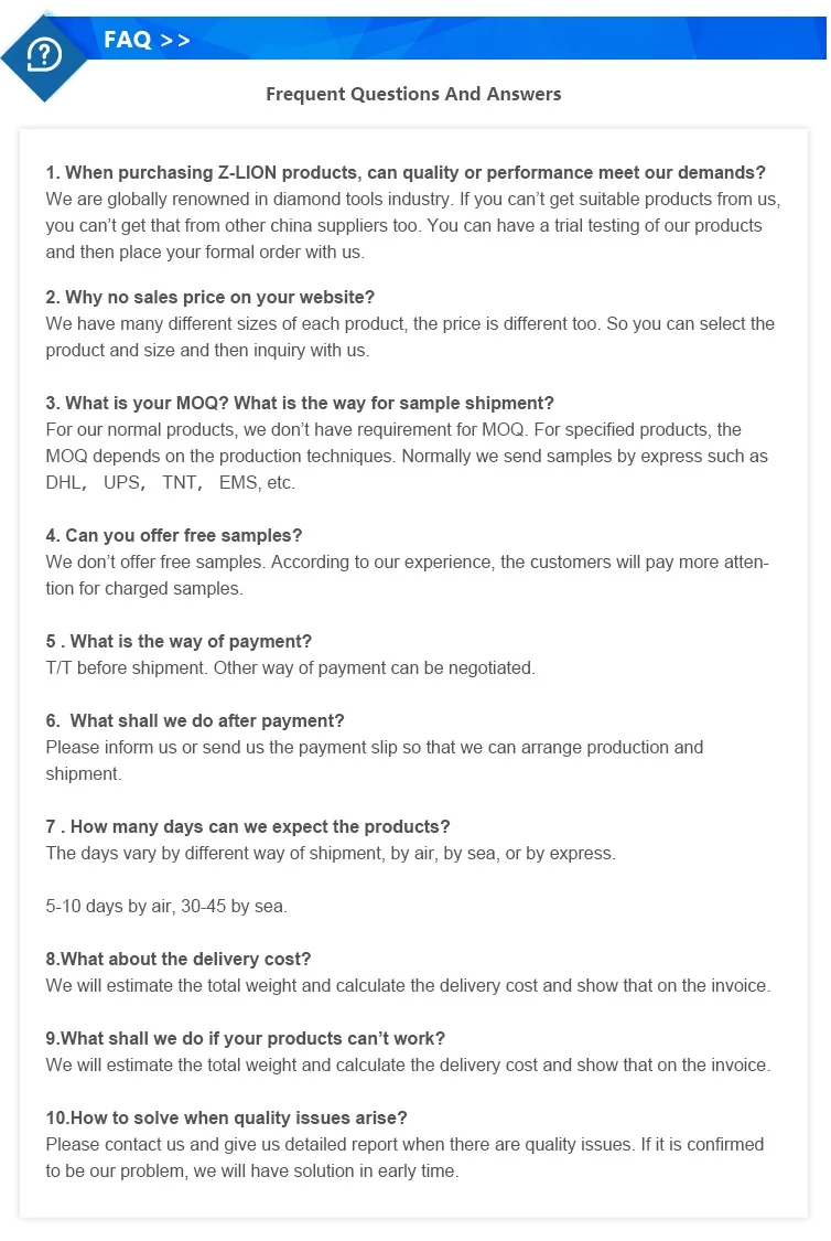
FAQ